Every consumer shares the common expectation of “reliable operation” when purchasing a product. Imagine spending a significant amount of money only to discover the item is faulty from the get-go. Naturally, you would be livid and want to make your dissatisfaction known to the manufacturer.
This customer dissatisfaction will have a major impact on the business’s reputation, which is why many manufacturers develop stringent testing methods to ensure they can deliver the highest quality product to their end-users. And this process is no different in the semiconductor industry.
However, if you are a newcomer, you might not be aware of the testing protocols and terms utilised in this industry. But fret not! We are here to help clarify things. Let us share everything you need to know about the burn-in testing process.
What does the burn-in test process entail?
So what is a burn-in test? Well, ‘burn-in’ refers to a process where semiconductor components are stress tested in extreme conditions to identify any early defects caused by poor materials, design, or manufacturing. These assessments are conducted with the aid of burn-in systems, with specific test conditions meant to mimic real-world scenarios.
During a burn-in test, the semiconductor components are pushed beyond the limits they are exposed to in reality to allow for additional headroom. The goal is to trigger possible failures that may occur during usage so that improvements can be made to minimise these situations from happening in real-time. Hence, manufacturers can rest easy knowing they have a robust end-product available to users.
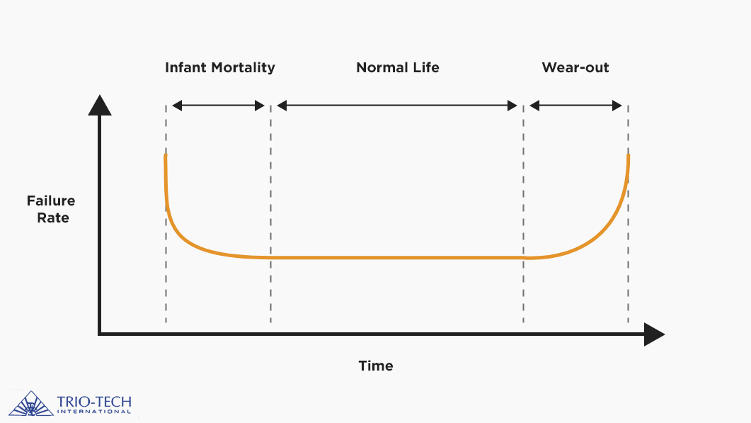
Usually, semiconductor components experience high failure rates during the early stages of operational life – we refer to this as infant mortalities. This is best illustrated by a Bathtub Curve (pictured above).
During a burn-in test, the temperature is elevated to accelerate and detect any failing mechanism. Subsequently, manufacturers can work on eliminating the causes of these early device failures. As a result, the failure rate decreases over time, and components are expected to operate normally in their useful life phase. This encapsulates the burn-in process.
What is a burn-in board?
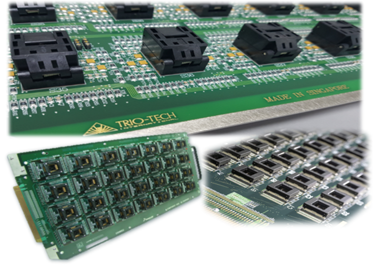
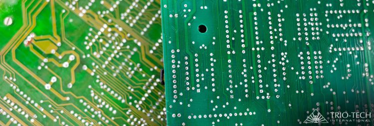
As you continue your research, you will undoubtedly have come across the term “burn-in board”. However, this term may have you scratching your head as a layman. So what exactly is a burn-in board? Well, a burn-in board refers to a printed circuit board (PCB) used in the burn-in process.
The semiconductor components are added to this board before they are exposed to extreme heat to highlight any failures. Once the burn-in test is completed, technicians will analyse the results to ensure that every component is functioning normally and within the correct parameters.
When conducting a burn-in test, temperatures usually range from 125°C – 250°C. In specific conditions, the temperature may even reach 300°C. Therefore, it is essential to make sure the burn-in board you utilise is made of high-grade materials, such as polyimide and stainless steel, to withstand these high temperatures.
What are the types of burn-in processes available?
Now that you are familiar with the burn-in process and what a burn-in board refers to, let us explore the common burn-in testing systems utilised by manufacturers to identify defects in their semiconductor components.
Static burn-in
Under a static burn-in system, the testing devices are mounted to the burn-in board sockets. Subsequently, they are placed in a burn-in oven where they are exposed to elevated temperatures and voltage applied over an interval of 12 to 24 hours. After cooling, the devices undergo a series of functionality tests to detect any defects that may be present within the components.
Although the static burn-in system is helpful in specific testing scenarios, it also has its limitations. No input signals are applied during the testing phase, so it does not provide an in-depth view of component reliability. However, the test’s simplicity and low cost serve as an ideal thermal test to mimic storage at extreme temperatures.
Dynamic burn-In
In a dynamic burn-in system, input signals are applied to each component while the burn-in board is subjected to extreme voltage and temperatures. This testing process provides a more comprehensive view of the component’s reliability. The output of each unit can be observed during the testing phase, giving manufacturers an insight into which parts are most susceptible to failure.
Regardless of the burn-in testing system you ultimately opt for, there is no denying the test’s importance in evaluating a semiconductor device’s reliability. So if you are on the lookout for an experienced company that can provide you with reliable burn-in testing services, do not hesitate to contact us today to learn how we can help you!