PART 1 – INTRODUCTION
No matter where we go, we are constantly surrounded by technology. In fact, our smartphones have become an indispensable tool in our everyday lives. You will be hard-pressed to go a day without utilising this device.
These various types of technologies all require an essential component – a semiconductor. Think of it as the brain of modern electronics. Similar to any electronic device, we need to ensure the reliability of this crucial component so that our equipment functions correctly.
So how do manufacturers enhance the probability of delivering the best product to end-users? Well, this is done through rigorous semiconductor testing. And one of the most common and vital testing protocols is a burn-in test. This testing process is designed to detect early failures in components and reduce the potential for defects and failures when in use.
Whether you are familiar with the intricacies of burn-in testing or not, there is no denying its importance. But if you fall into the latter category, fret not! This guide will outline everything you need to know about the process.
PART 2 – WHAT YOU NEED TO KNOW ABOUT BURN-IN TESTING
2.1. The purpose of conducting burn-in testing for semiconductors
Consumers pay top dollars for their electronic devices. The last thing they want is for the product to malfunction within a few years of their purchase. While there is no way to guarantee a 100% success rate, conducting a burn-in test to replicate an actual field stress environment can help reduce failure rates.
These burn-in tests, performed over a significant sample size, allow manufacturers to gain a better understanding of how the semiconductors will perform in real-world applications. Any component that breaks down during the test is discarded.
Through this elimination process, manufacturers can minimise the number of defective semiconductors they ship to their clients. This method increases the probability of an electronic device performing to a consumer’s expected levels of reliability. As such, burn-in testing is essential to ensure quality control of the production line.
2.2. How is a burn-in test performed?
As we have discussed, conducting a burn-in test helps reduce the number of devices that will fail prematurely. But how is the entire process carried out? This is accomplished by placing the semiconductor components under specific high-stress conditions to replicate enhanced field environments. Through this procedure, manufacturers can identify and eliminate defective parts.
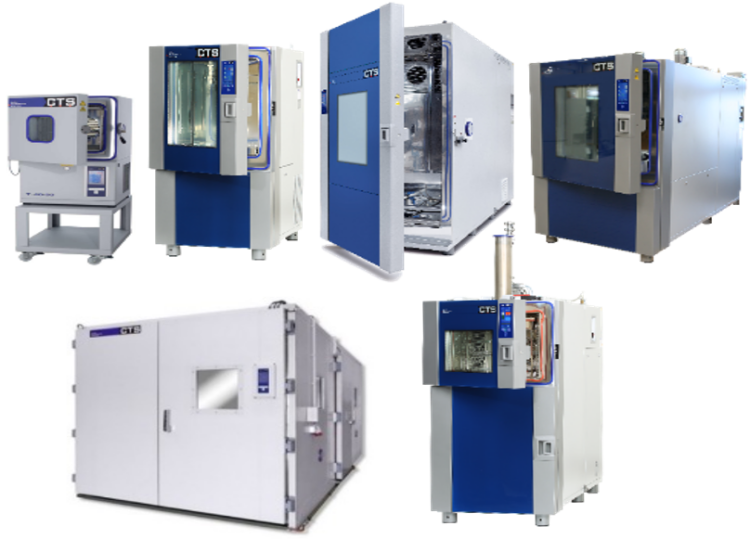
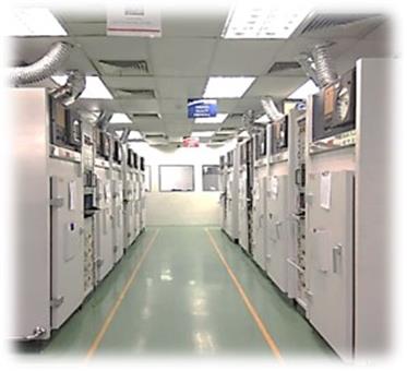
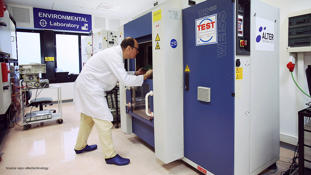
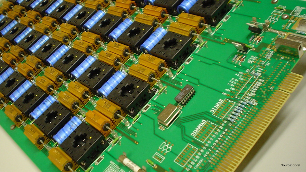
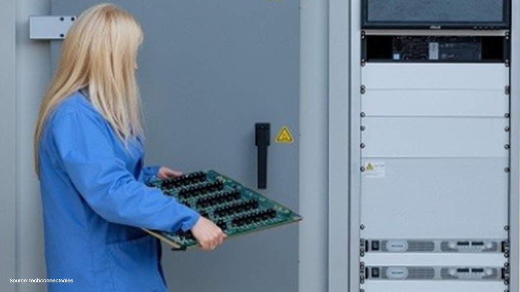
During the test phase, the semiconductor components are fixed onto a burn-in board before being placed in a burn-in system, like an environmental chamber. In this chamber, the parts are stress-tested at or above the normal operating conditions to phase out any assemblies that break down before the rated lifetime of the semiconductors.
Depending on the test scenarios, these operating conditions can include exposing the semiconductor components to extreme temperatures, varying voltage/current, high operating frequency, or any other conditions that are classified as an upper limit.
The above factors serve as enhanced stressors to induce failure in these devices. By subjecting the parts to carefully calibrated harsh conditions in a controlled environment, technicians can identify poor-performing components without affecting the useful life of the quality ones.
The goal of these burn-in tests is for manufacturers to gather sufficient data to form a bathtub curve (example below) and reduce the semiconductor failure rate.
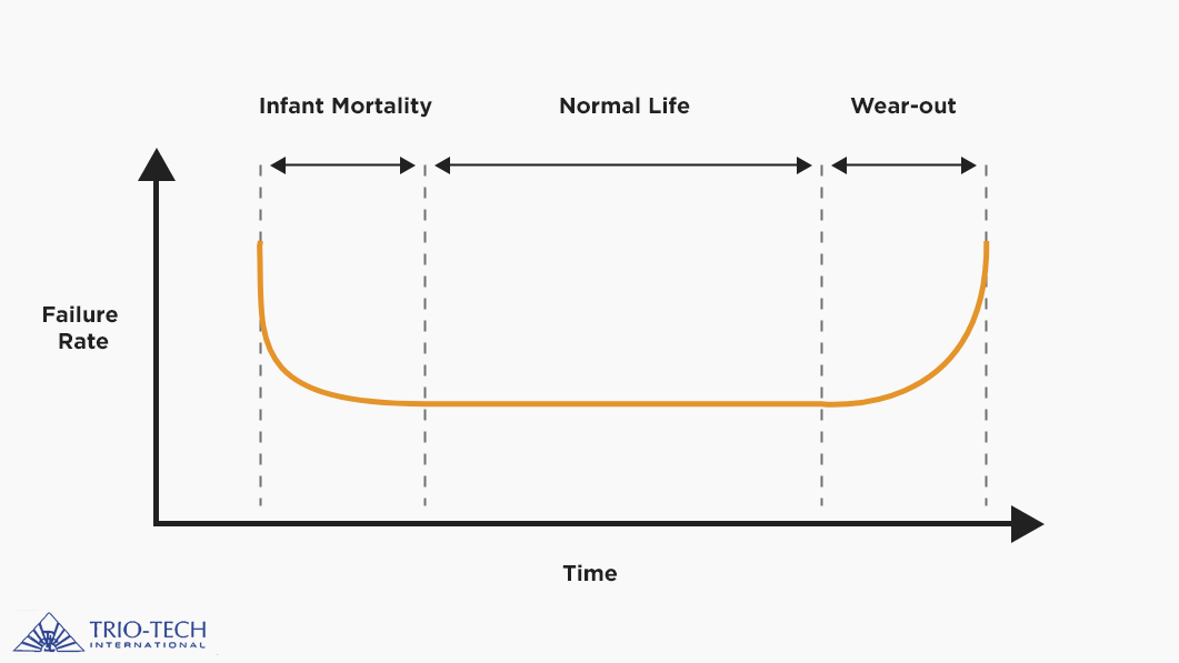
During the initial testing phase – classified as the infant mortality period – many semiconductors experience early component failure. These breakdowns are often a result of manufacturing defects which are becoming more common due to aggressive technology scaling and increased circuit complexity.
The root cause of these defects can be identified as conductor failures, electromigration, dielectric failures, metallisation failures, and many more. These defects cannot be discovered via conventional quality-assurance tests as these types of faults are often dormant and may surface randomly during a device’s life cycle. Therefore, the semiconductor components need to undergo intensive testing for such problems to manifest as failures.
However, despite the failure rate dropping over time, the results during the infant mortality period are undesirable as there is still a significant amount of breakdowns occurring within a short span of time. Delivering the semiconductors at this stage will result in customer dissatisfaction and steep warranty expenses.
The hope is that through feedback gathered from the burn-in tests, the manufacturing process can be enhanced, leading to a lower failure rate. While the components may still break down over time, the aim is to ensure that these failures generally occur in the normal life phase of the product’s lifespan. If the devices last until they reach the wear-out stage, that will be ideal.
Theoretically, a failure can still occur at random during the normal lifespan of a semiconductor. However, these problems generally surface at a relatively constant rate when measured over a significant period of time. As a result, it may be treated as a non-issue and written off as a product reaching the end of its lifespan.
Nevertheless, these problems will still incur warranty expenses for the manufacturers. Therefore, they will want the bottom of the bathtub curve (the failure rate) to be as low as possible. Any wear-out failures that occur during the expected useful lifespan of the semiconductors will also have to be addressed before the products are ready to be shipped to clients.
Another crucial detail to note is that burn-in tests are typically carried out on deliverable products. As such, these assessments are less intensive than accelerated life testing. The time these semiconductor components spent in burn-in is also lesser than in an ALT test. After all, manufacturers do not want to impact the lifespan of their products.
The temperatures used in a burn-in test generally reach 150 degrees Celsius or less, and the test increments can span between a few hours to a few days depending on the testing requirements. This is in contrast to an ALT test, where the devices are exposed to temperatures up to 300 – 400 degrees Celsius for a significant time – thousands to tens of thousands of hours – to reach the component’s failure point.
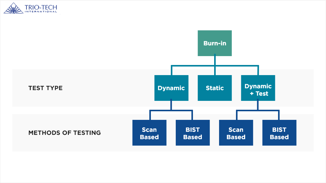
2.3. Types of burn-in tests
Now that you have a better understanding of the burn-in test process, you may be wondering if there are any differences in the test type and method of testing. The answer is yes! The type of burn-in test utilised during the testing process will depend on your requirements.
If you are unsure which testing method best matches your needs, allow us to break down the three different types of tests available and their advantages and disadvantages so that you can make an informed decision.
Static testing
During a static burn-in test, extreme temperatures and voltages are applied to each part without operating or exercising each component. This process is relatively straightforward. The probes simply need to be installed into an environmental chamber before the chamber is raised to the prerequisite temperature. Subsequently, the desired voltage is applied to the semiconductor components. Many manufacturers opt to utilise static burn-in due to its low cost and simplicity.
However, this testing method does not provide manufacturers with a comprehensive view of the component reliability. This is because the static voltage applied during the test does not activate all the nodes in a semiconductor. It is only useful as a thermal test to gauge the condition of the semiconductors when they are stored at extreme temperatures.
Dynamic testing
During a dynamic burn-in test, a burn-in system will apply multiple electrical stimuli to each component while the semiconductors are exposed to high temperatures and voltages. This testing method offers a more sweeping view of component reliability since it offers manufacturers the ability to stress more internal circuits, causing additional issues to surface.
The outputs can be monitored during the assessment, providing manufacturers with a better understanding of which points on the board are most vulnerable to failure. But there is also a drawback to this method. Dynamic burn-in cannot completely simulate the real-world applications of the semiconductor, so not all the circuit nodes will be stress-tested.
Dynamic burn-in with test
A dynamic burn-in with test process allows technicians to monitor the device output at various points in the burn-in process, confirming that each component is being exercised. This method is suitable for manufacturers looking to quickly determine burn-in “fallout” as a function of time, allowing the burn-in process to be terminated at an optimal point.
Additionally, this testing method allows manufacturers to identify components that will fail under marginal conditions but not at the device’s usual operating point. By detecting and eliminating these faulty devices during the testing phase, they can improve their product quality significantly.
Normally, most manufacturers will utilise a combination of static and dynamic burn-in tests to achieve the best results. After all, the performance data collected from these assessments are crucial in enhancing manufacturing processes. Therefore, it is beneficial to be more comprehensive in your testing, even if the costs are higher.
At the end of the day, the aim of implementing a burn-in system is to ensure increased visibility and insight into how the manufactured semiconductors will perform under stress. Each test phase should produce more statistically meaningful data, painting a clearer picture of the probability of failures for these devices. The data can prove to be helpful in dramatically improving product yield and enhancing the manufacturing process to create higher-quality semiconductors.
For manufacturers seeking a more comprehensive evaluation of their products, we will recommend pairing burn-in testing with other reliability test services. To ensure the reliability of semiconductors, various new processes have been developed which are used as alternatives or along with burn-in testing.
The notable processes include:
- Accelerated environment stress tests
- PC – Preconditioning
- Autoclave or Pressure cooker test
- THB – Temperature Humidity Bias
- HAST system – Highly Accelerated Temperature and Humidity Stress
- uHAST system – Unbiased Highly Accelerated Stress
- HTRB system – High Temperature Reverse Bias
- HSTL system – High Temperature Storage Life
- HVST system – High Voltage Stress Test
- Accelerated lifetime simulation tests
- HTOL testing – High Temperature Operating Life
- ELFR testing – Early Life Failure Rate
- NVM Endurance and Data Retention
- Die fabrication reliability tests
- Electro-migration
- Time Dependent Dielectric Breakdown
- Hot Carrier Injection
- Negative Bias Temperature Instability
- Stress Migration
- Environmental stress screening
- Temperature Cycling
- Thermal Shock
- Power Cycling
- Environmental Conditioning
2.4. What are the effects of burn-in testing?
There is no denying the effectiveness and accuracy of a burn-in test. This assessment allows manufacturers to check the performance of their products and identify hidden defects before they are shipped out to clients. But despite the benefits this process brings to the table, it also carries several disadvantages.
While these drawbacks should not dissuade manufacturers from conducting burn-in testing, as it remains a vital quality-assurance process, it is still necessary for businesses to be aware of the advantages and disadvantages. Let us share what these perks and drawbacks are.
Advantages of burn-in testing
A burn-in test remains the best way for manufacturers to screen and detect any high potential failures in their products. This is especially crucial for devices that are required to operate in extreme environments where failure is not permitted – such as the medical or military industry.
As the test looks to simulate real environmental conditions that other testing methods cannot replicate, it is the ideal gauge for manufacturers to check how their products will function during real-world applications.
Furthermore, they can rest assured that the semiconductor components that survive rigorous testing are high-quality parts free of latent defects. Therefore, they are safe to be integrated into the final product assembly. This ensures greater product reliability, which translates to better customer satisfaction.
Disadvantages of burn-in testing
While a burn-in test remains an ideal method to detect any flaws in a semiconductor, the total life span of the product may be affected by this assessment. The product’s useful life cycle may not be impacted, but other elements, such as the device stress distribution, efficiency, electro-static discharge (ESD), and competency to electrical-over-stress (EOS), are compromised. This is due to the components’ prolonged exposure to extreme temperature and voltage during a burn-in test.
Additionally, the semiconductor components that were assessed during the burn-in tests may degrade over time, necessitating a replacement. This will increase the cost of maintenance for these devices in the future. Another factor to note is that a burn-in test can often be time-consuming and labour-intensive. As such, manufacturers need to plan ahead of time to ensure every component can be thoroughly tested while meeting delivery deadlines.
2.5. What is the difference between a burn-in test, a highly accelerated life test, and a highly accelerated stress screening?

The world of electronics testing is brimming with its own technical terminology, which can be overwhelming to the uninitiated. Aside from the term “burn-in test”, you might have heard about other reliability test services, such as highly accelerated lift test and highly accelerated stress screening. But what do these terms mean? And how do they differ from a burn-in test?
Let us touch on the highly accelerated life test (HALT) first, as it shares many similarities to a burn-in test. In fact, a burn-in test can be considered a type of HALT. This is because HALT is not a specific test but rather a type of testing methodology.
Similar to burn-in testing, an HALT is generally conducted during the early stages of a product’s development. The test is intended to detect design flaws in the device by subjecting it to extreme conditions and accelerating its life cycle. The units that fail the assessment are identified and improved upon to eliminate any weaknesses detected during the HALT.
In contrast, a highly accelerated stress screening (HASS) is only conducted on a product after its general design is agreed upon and it has already been developed. Using the data gathered from previous HALTs as a guideline, an HASS is designed to apply further stresses to the device to ensure consumers do not receive defective products or units that malfunction quickly. However, these stress tests are limited to avoid impacting the product’s life cycle.
Despite several differences between an HALT and HASS, both methodologies consist of the same three specific types of tests – temperature profiling, humidity profiling, and vibration profiling.
Temperature profiling is conducted to identify the minimum and maximum temperatures under which the device remains useable. Humidity profiling, meanwhile, specifically tracks how the product reacts to extreme humidity. Lastly, vibration profiling exposes the unit to mechanical stress to assess its durability. This test is done to ensure the product can survive the rough treatment that may occur during transportation.
After learning more about HALTs and HASSs, you have probably noticed that a burn-in test can be classified as either an HALT or HASS since it counts as temperature profiling. It just depends on when the test is carried out during the product’s development cycle. However, despite their similarities, we generally distinguish these terms separately. When someone talks about conducting an accelerated life test, they are referring to more intense, rigorous, and prolonged testing compared to burn-in testing.
PART 3 – THE IMPORTANCE OF BURN-IN TESTING
After taking a deep dive into the ins and outs of a burn-in test, it is obvious why this assessment is critical in the electronics industry. And its importance will only continue to grow as semiconductor technology advances. With semiconductors being a crucial component in numerous devices, burn-in testing has become an essential procedure for quality assurance.
It remains the best option for manufacturers to maintain a stellar company reputation and keep up with semiconductor market standards. After all, identifying and reducing early failures is the first step to ensuring product reliability. This way, only the semiconductors with a low probability of early failure will be released, thereby ensuring that businesses can deliver high-quality and reliable products to consumers constantly.
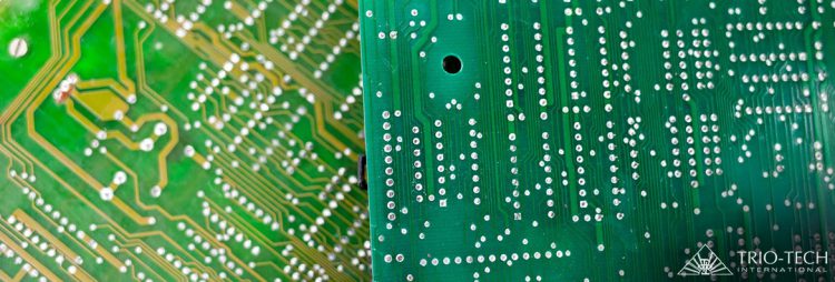
It is also worthwhile to note that semiconductor components are not the only devices applicable for burn-in testing. Printed circuit boards (PCBs), integrated circuits (ICs), and processor parts are also tested under burn-in conditions to ensure their reliability.
PART 4 – CONCLUSION
As technology continues to advance at a rapid pace, manufacturers need to adapt to continue meeting industry standards. With new technologies – like the evolution of 5G – necessitating quality semiconductors, the electronics industry requires instant feedback to quickly identify failure characteristics and improve its manufacturing processes to meet this demand. And burn-in testing can provide this missing link!
However, while burn-in tests remain a vital cog in the wheel, it is only one process among many in ensuring product reliability. The onus is still on companies to drive reliability through continuous process improvement. After all, a burn-in test will only help identify problems, but it does not guarantee a quality product. Factors such as material quality, manufacturing process control, and quality workmanship should continue to be the foremost priorities for businesses.
Nevertheless, burn-in testing remains a cornerstone for providing semiconductor manufacturers with accurate updates on their product reliability. It enables businesses to monitor and benchmark any process or technology changes and offers consumers quality assurance when they purchase a product. With semiconductors remaining a vital component of all electronics, the demand for burn-in testing is likely to remain.
At Trio-Tech International, we are one of the leading providers of semiconductor testing and burn-in services in Singapore. We offer a comprehensive list of reliability test services, including automotive burn-in tests. With over 40 years of experience in the industry, our team of experts can provide your business with quality and detailed findings on the performance of your products. This information will be helpful in improving your product reliability.
Furthermore, all of our testing facilities are ISO9001, ISO14000, ISO17025, and DSCC certified. You can rest assured that our operating policies and procedures fulfil the stringent international standards for consistency and reliability. Do not hesitate to contact us today to learn more about how we can help you with your product testing.